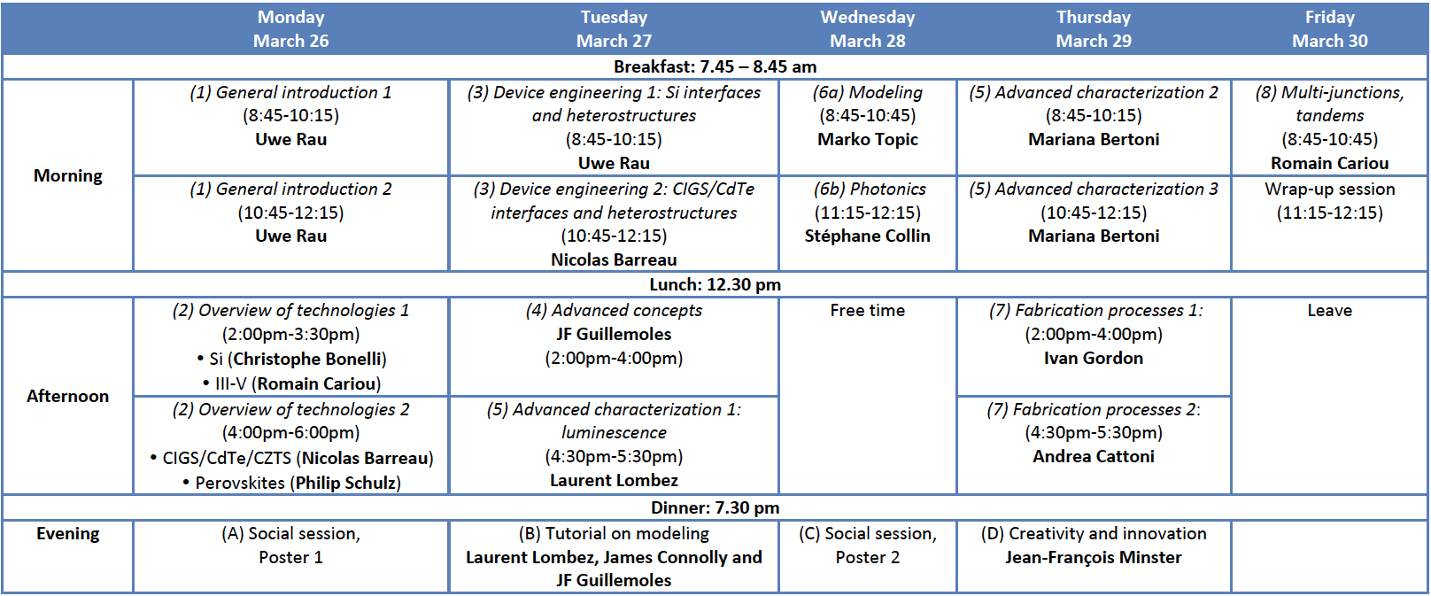
The program is now available (pdf):
Program:
- General introduction 1 & 2 (3h), Uwe Rau
- Overview of technologies 1 & 2 (3h30):
- Si (1h), Christophe Bonelli
- III-V (30mn), Romain Cariou
- CIGS/CdTe/CZTS (1h), Nicolas Barreau
- Perovskites (1h), Philip Schulz
- Device engineering 1 & 2 (3h):
- Si interfaces and heterostructures (1h30), Uwe Rau
- CIGS/CdTe interfaces and heterostructures (1h30), Nicolas Barreau
- Advanced concepts (2h), JF Guillemoles
- Advanced characterization (4h):
- 1: Luminescence (1h): Laurent Lombez
- 2 & 3 (3h): Mariana Bertoni
- Modeling & Photonics (3h)
- Modeling (2h): Marko Topic
- Photonics (1h): Stéphane Collin
- Fabrication processes (3h):
- 1 (2h): Ivan Gordon
- 2 (1h): Andrea Cattoni
- Multi-junctions, tandems (2h): Romain Cariou
Evening sessions:
- Social session, Poster 1
- Tutorial on modeling: Laurent Lombez, James Connolly and JF Guillemoles
- Social session, Poster 2
Creativity and innovation, Jean-François Minster(canceled, 24/03/2018)
Lecture descriptions:
(1) General introduction
Keywords: thermodynamics approach, theoretical limits, fundamental working principles…
Description: The goal will be to introduce the general principles of solar cell operation using different approaches: a thermodynamic point of view, and a description of the basic operating principles closer to an engineering approach.
(2) Overview of technologies
Keywords: c-Si, CIGS, CdTe, CZTS, III-V, perovskite,…
Description: The overview of the different technologies will focus on the description and limits of conventional devices, and the main trends of current researches.
(3) Device engineering: interfaces and heterostructures
Keywords: Carrier collection, passivation, heterostructures, interfaces, contacts,…
One part on Si heterostructures that could include oxides as collecting layers.
One part on interfaces and heterostructures in thin-film photovoltaics.
Description: For efficient carrier collection, a special care should be devoted to the design and realization of the passivation and contact layers. Heterostructures based on wide-bandgap semiconductors and TCO are at the forefront of recent advances and designs of both silicon and thin-film solar cells. The role of interfaces is a key.
(4) Advanced concepts
Keywords: Beyond Shockley-Queisser without stacking cells! Hot-carriers, IBSC, up-/down-conversion and spectral shifting, multi-carrier generation…
Description: Efficiency of single junction cell is limited by the SQ limit. We will present original physical concepts to overcome this limit without using MJ cells. We will see how it is possible to reduce the two main losses in PV conversion (transparency and heat dissipation) as well as how one can do photon management to modify the sunlight.
(5) Advanced characterization
Keywords: Overview of the main characterization techniques. Nanoscale characterization. AFM, Luminescence, EBIC/LBIC, XPS, NanoAuger,…
Description: A general description of fundamental characterization techniques and methods will be given. We will then focus the lecture on advanced methods based on luminescence signal and techniques allowing characterization at a micro and nano-scale.
(6a) Modeling
Keywords: Multiscale modeling. Device and optical modeling.
Description: This lecture will be focused on device and optical modeling. A special care will be given to multiscale modeling, and to the domain of validity of each method. Initiation of device modeling with an evening practical work will be proposed; it will illustrate the working principle of a PV cell.
(6b) Photonics
Keywords: Theory of light trapping. Random scattering. Periodical patterns. Ultrathin solar cells.
Description: Sunlight absorption is a prerequisite for any solar cell. The goal of this lecture is to describe the different strategies for light trapping, from a theoretical and practical point of view. Applications to ultrathin solar cells will be reviewed.
(7) Fabrication processes
Keywords: Bottom-up and top-down techniques. Micro- and nano-fabrication technologies.
Description: A general introduction to solar cell fabrication will be presented, and bottom-up and top-down techniques will be detailed. Beyond conventional fabrication techniques, micro- and nanostructures can be implemented in solar cell devices to improve light management and carrier collection. The lecture will present a selection of unconventional scalable and cost-effective micro- and nano-fabrication technologies and their application in PV cell fabrication.
(8) Multijunctions, tandems on Si
Keywords: III-V tandems for CPV, III-V on Si and other/Si.
Description: Multi-junction (MJ) solar cells are the only architecture that has overcome the Shockley-Queisser (SQ) limit, to date. III-V semiconductors are at the core of most multi-junction devices, and serve as a model for high-efficiency solar cells. Tandem structures on Si are considered as the most promising approach to push the limits of conventional silicon solar cells. The different options (III-V/Si, perovskite/Si, CIGS/Si) will be described and discussed.


Physics of Solar Cells: from basics to nanoscience (25-30 March 2018)
Les Houches School of Physics


