


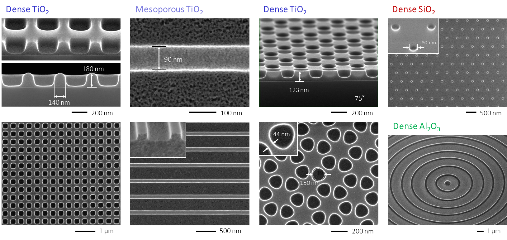
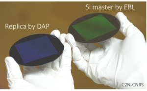
To support the activities on photovoltaics we develop low-cost and large surface area nanofabrication technologies based on Soft Nanoimprint Lithography (NIL) [Cattoni2011][Dalstein2016][Graczyk2018][Cattoni2018][Bottein2018]. Soft NIL uses cheap and flexible stamps replicated from a single and expensive silicon master fabricated by electron beam lithography (EBL). The flexibility of the polymeric stamp ensures contact with the surface substrate on large surfaces at low pressures, even on curved or flexible substrates. In particular we developed a process called Degassing Assisted Patterning (DAP) for the replication of nanostructures in organic UV-curable resists and inorganic dense or mesoporous sol-gel derived films (TiO2, SiO2, Al2O3, IrO2).
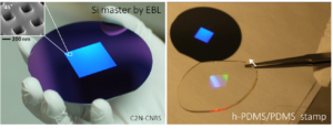
The silicon master mold is first fabricated at C2N by electron beam lithography (100 KV Vistec EBPG 5000+) and dry etching. An anti-sticking treatment is performed using a silanes-based functionalization.
The polymeric stamp (Ormostamp or PDMS-based) is then replicated by molding and is also treated with an anti-sticking treatment.
DAP – The PDMS-based stamp is first degassed in a dessicator for 5 minutes. Due to its high porosity, PDMS has a high gas solubility that obeys Henry’s law, so that the equilibrium concentration of gas dissolved in PDMS is proportional to the partial pressure of the gas around the PDMS. Once degassed and brought back to atmospheric pressure, the PDMS stamp behaves like a sponge by absorbing air to reach a the new equilibrium with a time constant of minutes. For this reason, after molding the PDMS stamp onto a spin-coated substrate with a UV-curable resist (or sol-gel hybrid film), eventual macroscopic air bubbles surrounding defects or induced by imperfect molding are removed within few seconds through the diffusion of air in the degassed stamp. In the same way, the pressure difference assists the capillary forces during the filling of the stamp protrusions: the air trapped in the stamp protrusion is aspired inside the stamp and replaced by the resist. When using sol-gel hybrid film, the degassed stamp also quickly removes the solvents. Before the demolding of the stamp, the resist is stabilized by UV-light exposure while the sol-gel is stabilized at about 100 °C for few minutes. Either dense or mesoporous hierarchical nanopatterns can be obtained by tuning the composition of the initial sol-gel solution.
Advantages of DAP:
- High resolution up to 20 nm
- Cost effective! No imprinter machine
- No pressure → no long-range deformations
- Bubble-defects-free
- Fast! The whole embossing process is performed in less than 2 min
- Large surface area parallel replication
Collaborations: Marco Faustini and Cedric Boissiere (Laboratoire de Chimie de la Matière Condensée de Paris, Sorbonne University)