


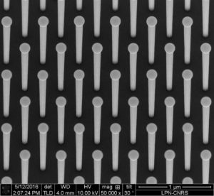
III–V nanowires (NWs) belong to next-generation solar materials, which can offer efficiencies far beyond Si technology. The direct growth of III-V nanowires on Si is of particular interest for low-cost tandem solar cells. In close collaboration with the material department, different approaches are currently explored at C2N based on the direct growth of ordered arrays of self-catalyzed III-V nanowires on Si by molecular beam epitaxy using the Vapor-Solid-Liquid method.Recently, we addressed and solved several issues related to the selective growth of ordered NWs arrays on Si(111):
> we demonstrated a high and reproducible yield (> 95 %) of vertical NWs without parasitic deposits on the mask,
> by measuring and modeling the growth dynamics of these ordered arrays, we showed that Ga atoms impinging on the mask participate to NW growth via a specular or lambertian reemission from the mask rather than via their diffusion on the mask surface [Oehler2018],
> we developed a method to determine the doping level of III-V semiconductors at the nanoscale using cathodoluminescence and generalized Planck’s law modelling [Chen2017b].
Both axial and radial junction NWs are fabricated using GaAs and ternary (GaAsP and AlGaAs) alloys [Himwas2017]. First NW solar cells on Si have been fabricated successfully. The optimization of the solar cell fabrication process is on-going.
This research topic is carried out in close collaboration with IPVF, and supported by the NANOCELL and HETONAN ANR projects.