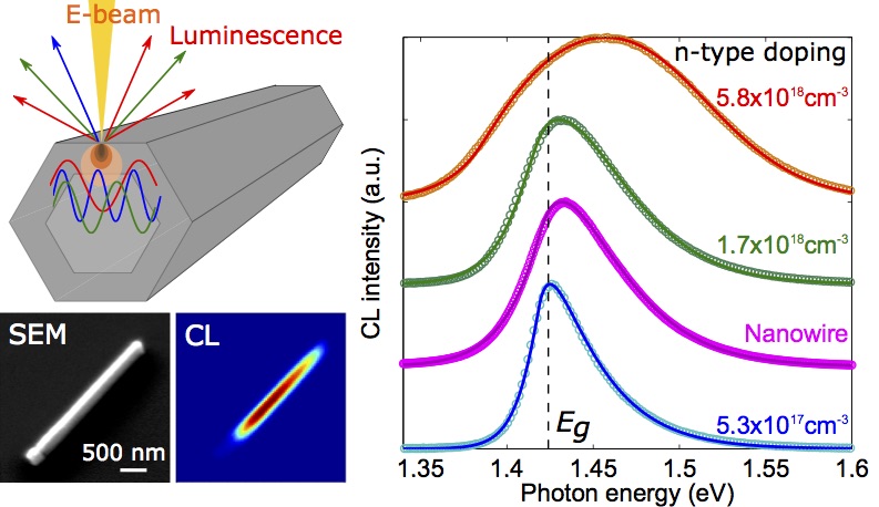
We present an effective method of determining the doping level in n-type III–V semiconductors at the nanoscale. Low-temperature and room-temperature cathodoluminescence (CL) measurements are carried out on single Si-doped GaAs nanowires. The spectral shift to higher energy (Burstein–Moss shift) and the broadening of luminescence spectra are signatures of increased electron densities. They are compared to the CL spectra of calibrated Si-doped GaAs layers, whose doping levels are determined by Hall measurements. We apply the generalized Planck’s law to fit the whole spectra, taking into account the electron occupation in the conduction band, the bandgap narrowing, and band tails. The electron Fermi levels are used to determine the free electron concentrations, and we infer nanowire doping of 6 × 10^17 to 1 × 10^18 cm-3. These results show that cathodoluminescence provides a robust way to probe carrier concentrations in semiconductors with the possibility of mapping spatial inhomogeneities at the nanoscale.
For more information, please read our article recently published in Nano Letters.
Reference:
- Determination of n-type doping level in single GaAs nanowires by cathodoluminescence, Hung-Ling Chen, Chalermchai Himwas, Andrea Scaccabarozzi, Pierre Rale, Fabrice Oehler, Aristide Lemaître, Laurent Lombez, Jean-François Guillemoles, Maria Tchernycheva, Jean-Christophe Harmand, Andrea Cattoni, and Stéphane Collin, Nano Letters 17, 6667-6675, 2017.


