

In a series of two articles recently published in Phys. Rev. Applied, we show how cathodoluminescence mapping can be used to provide a contactless, quantitative assessment of active doping at the nanoscale. The method is applied to n-doped and p-doped GaAs nanowires.
Doping, a fundamental property of semiconductor devices can be measured at the nanoscale thanks to long term developments made in the framework of the IPVF-C2N partnership. In a twin papers published in Phys. Rev. Applied, we take advantage of the signature of the charge carrier concentration in the luminescence of semiconductors.
In the first article, we analyze a wide range of p-type and n-type GaAs thin films with carrier concentrations spanning from 2×10¹⁷ to 1×1019 cm−3. The luminescence spectra are fitted with the generalized Planck law and with a refined absorption model that takes into account the bandgap narrowing and the band filling induced by the doping. They are used as references to fit and calibrate cathodoluminescence (CL) measurements, and to provide a rigorous method for the quantitative assessment of p-type and n-type carrier densities by CL.
In the second article, we apply this method to analyze the doping concentration profiles in single GaAs nanowires (NWs). High-resolution maps of the hole concentration demonstrate the homogeneous doping in pure zincblende segments of GaAs:Be NWs. For Si-doped GaAs NWs, the electron Fermi level and the full width at half maximum of low-temperature CL spectra are used to assess the electron concentration to approximately 3 × 10¹⁷ to 6 × 1017 cm−3. These findings confirm the difficulty in obtaining highly doped n-type GaAs NWs, maybe due to doping compensation.
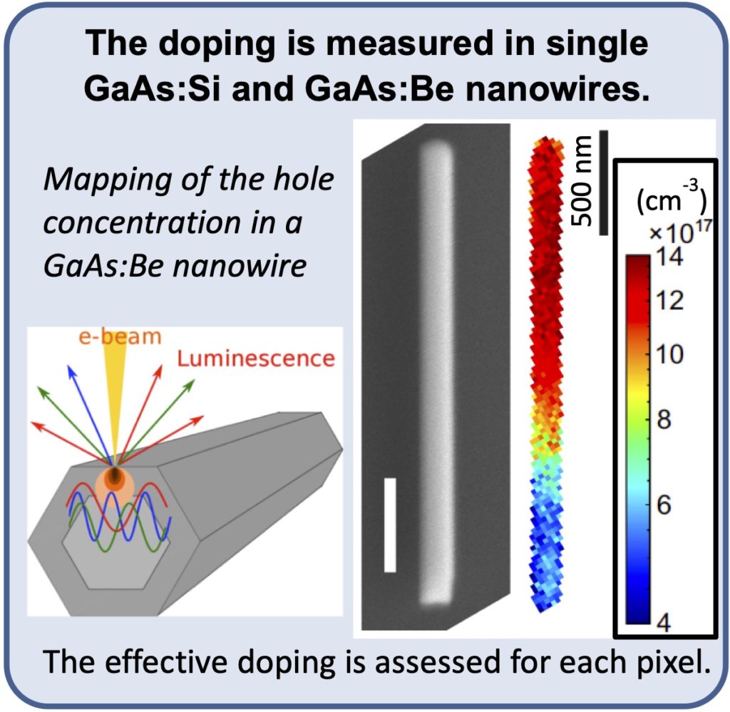
Overall, these results show that high-resolution hyperspectral CL mapping is an efficient tool for contactless assessment of carrier densities at the nanoscale. The method can be extended to other semiconductors and applied to numerous nanostructures and devices.
References:
• Quantitative Assessment of Carrier Density by Cathodoluminescence I. GaAs thin films and modeling, Hung-Ling Chen, Andrea Scaccabarozzi, Romaric De Lépinau, Fabrice Oehler, Aristide Lemaître, Jean-Christophe Harmand, Andrea Cattoni, and Stéphane Collin, Phys. Rev. Applied 15, 024006, 2021.
• Quantitative Assessment of Carrier Density by Cathodoluminescence II. GaAs nanowires, Hung-Ling Chen, Romaric De Lépinau, Andrea Scaccabarozzi, Fabrice Oehler, Jean-Christophe Harmand, Andrea Cattoni, and Stéphane Collin, Phys. Rev. Applied 15, 024007, 2021.